The financial press is currently swooning over South Korea’s staggering $880 billion mega-cluster initiative. Headlines present it as a masterstroke of economic warfare, a definitive blueprint to secure dominance over global supply chains until 2047. The collective consensus is clear: throw enough capital at the ground, and a self-sustaining silicon empire will automatically sprout.
It is a comforting narrative. It is also completely wrong.
This historic capital injection is not an offensive strategy. It is an act of sheer desperation. By committing nearly a trillion dollars to physical infrastructure, Seoul is doubling down on a twentieth-century hardware playbook to solve a twenty-first-century software crisis. They are building the world’s most expensive foundry network at the exact moment the value matrix of the tech economy is shifting permanently away from pure manufacturing.
The Subsidized Yield Illusion
The lazy assumption governing global industrial policy is that fabrication capacity equals geopolitical leverage. The United States has the CHIPS Act. Europe has its own state-backed funds. Korea is simply building the biggest one.
But capacity is not capability.
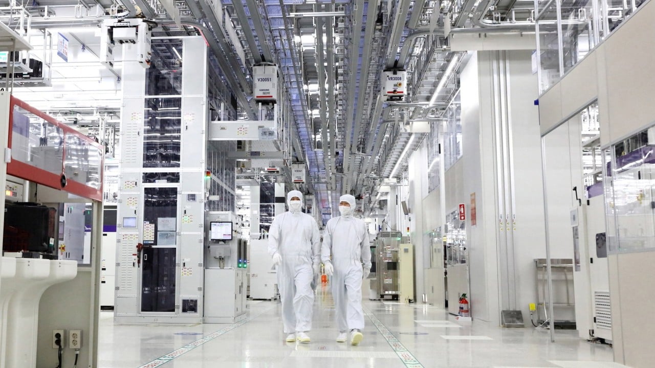
The competitor articles marvel at the sheer scale of the planned Yongin mega-cluster: 13 new fabs, three research facilities, and a projected output of 7.1 million wafers per month. What they fail to analyze is the structural rot beneath these numbers.
For three decades, Korea's tech dominance rested on memory chips—specifically DRAM and NAND flash. This is a highly cyclical, commoditized commodity business. Success requires massive capital expenditures and ruthless execution. Samsung and SK Hynix mastered this.
However, the current AI boom does not care about standard memory. It demands advanced logic chips and High Bandwidth Memory (HBM)—architectures where design, software optimization, and packaging dictate performance far more than raw silicon throughput.
When you look closely at the $880 billion figure, you realize it is almost entirely private capital from Samsung and SK Hynix, dragooned into a concentrated geographic zone via government tax incentives. It is an aggressive centralization of systemic risk. If a single geopolitical shock or supply disruption hits the Gyeonggi Province, the entire state apparatus collapses with it.
The Foundry Lie: Why You Cannot Just Buy Taiwan's Moat
The grand ambition of this investment is to challenge TSMC in the foundry space—manufacturing chips designed by third parties like Nvidia, Apple, and AMD.
Every industry insider knows the ugly truth: Samsung’s foundry division has spent the last five years bleeding market share to TSMC. Throwing hundreds of billions at new cleanrooms does not solve the fundamental issue holding them back: Yield and Trust.
In semiconductor manufacturing, yield is the percentage of functional chips produced on a single wafer. TSMC consistently achieves superior yields on advanced nodes compared to its competitors. This is not merely a function of having newer machines; it is a result of decades spent refining proprietary operational processes alongside global design firms.
More importantly, TSMC does not compete with its customers. It has a strict rule: "No chips of our own."
Samsung, conversely, is a massive conglomerate that builds its own smartphones, consumer electronics, and application processors. When an external design firm hands its most sensitive, proprietary chip blueprints to Samsung Foundry, it is handing intellectual property to a direct competitor in the end-market. No amount of state-subsidized infrastructure can erase that structural conflict of interest.
I have watched hardware executives blow through tens of millions of dollars attempting to migrate designs away from Taiwan to diversify their supply chains. They almost always crawl back. Why? Because TSMC’s real moat isn’t their physical machinery—it is the Open Innovation Platform (OIP) ecosystem. It is the software libraries, the design IP blocks, and the seamless integration with electronic design automation tools. Korea’s megafund treats this like a real estate problem. It is an ecosystem problem.
Dismantling the Premier PAA Myths
The public dialogue surrounding this investment is warped by fundamentally flawed assumptions. Let us dismantle them directly.
Does massive infrastructure funding guarantee AI dominance?
No. Hardware is merely the tax you pay to run AI models. The real value is captured at the software, algorithmic, and proprietary data layers. Building fabs does not magically create an ecosystem of AI engineers. Look at Japan in the late 1980s: they controlled over 50% of the worldwide semiconductor market through state-directed industrial policy. Yet, because they failed to capture the software architecture shift led by Microsoft and Intel, their hardware dominance evaporated within a decade. Korea is repeating this exact mistake, optimizing for silicon processing power while remaining entirely dependent on American software frameworks like PyTorch and Nvidia’s CUDA.
Can state subsidies offset the semiconductor talent shortage?
They cannot. You can build a state-of-the-art facility in two years, but you cannot breed a top-tier lithography engineer in less than ten. South Korea is facing a severe demographic collapse. The domestic talent pipeline is shrinking at an alarming rate. Engineering graduates are increasingly fleeing traditional hardware conglomerates for global software firms or finance. An $880 billion fund cannot buy human capital that simply does not exist on the open market. Without a massive, politically unpalatable overhaul of immigration laws to import foreign engineering talent, these new mega-fabs will sit understaffed or operate at sub-optimal efficiency.
The Bottleneck Nobody Wants to Mention: Power and Water
Let us look at the brutal mechanical reality of running a 7.1 million wafer-per-month cluster.
A single modern fab utilizing Extreme Ultraviolet (EUV) lithography machines consumes upwards of 100 megawatts of electricity per day. That is enough to power a medium-sized city. The planned Yongin cluster will require an estimated 10 gigawatts of constant, uninterrupted power.
South Korea’s current energy grid is heavily reliant on fossil fuels and vulnerable to supply shocks. Furthermore, the domestic political landscape makes building new high-voltage transmission lines incredibly difficult due to intense local opposition. The government promises to build nuclear reactors and liquefied natural gas plants specifically for the cluster, but the timelines for these energy projects are completely detached from the planned fab rollouts.
Then there is the water crisis. Chip manufacturing is an incredibly thirsty enterprise. Wafers must be rinsed with ultra-pure water between each of the hundreds of processing steps. A mega-cluster of this scale will require millions of tons of water daily. Korea's seasonal rainfall variance and limited river resources mean that providing this volume without destroying agricultural and municipal supplies is an environmental tightrope walk.
If the power flickers for even a fraction of a second, or if water purity drops by parts per billion, entire production runs worth hundreds of millions of dollars are instantly ruined. The competitor pieces talk about funding; they ignore physics.
The Actionable Pivot for Survival
If this monolithic investment is a misallocation of capital, what should Korea be doing instead?
The country needs to stop trying to beat TSMC at a game Taiwan won fifteen years ago. Instead, capital should be aggressively diverted toward the true blind spots of the global semiconductor supply chain.
- Monopolize Advanced Packaging: The physical limit of transistor shrinking (Moore’s Law) has effectively been reached. Future performance gains will come from Chiplets—binding multiple smaller chips together in a single package. Instead of building massive, capital-intensive front-end foundries, Korea should focus on dominating back-end advanced packaging and heterogeneous integration. It is lower capital expenditure, offers higher margins, and represents the true bottleneck of AI hardware delivery.
- Fund the Electronic Design Automation (EDA) Underbelly: The entire global chip industry relies on just three companies for the software used to design semiconductors (Synopsys, Cadence, and Siemens). This is a pure software monopoly with absurdly high margins. Breaking this triad or creating specialized, AI-native design automation tools would yield far more geopolitical leverage than a dozen generic manufacturing plants.
- Accept the Cost of Divestment: Policymakers must accept that some legacy memory manufacturing must be outsourced to lower-cost regions. Keeping low-margin production artificially alive on domestic soil through endless tax breaks simply drains resources away from high-value research and development.
This $880 billion plan is not a visionary leap forward. It is defensive architectural entrenchment disguised as progress. It assumes that the future of technology will look exactly like the past, only larger and more expensive.
History shows that when a state becomes obsessed with building monuments of steel and silicon rather than cultivating software and talent, it is usually a sign of an empire in decline. The money will be spent. The concrete will be poured. But when the dust clears, the true power centers of the technology world will still be defined by lines of code, not the square footage of cleanrooms.